Research
"Electronic properties of SiON/SiC(0001) surface ~ band-gap profile, Schottky contact ~"
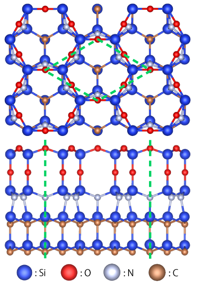
Silicon carbide (SiC) is a promising material in applications for electronic devices because of its large band gap and high thermal conductivity. However, it is hard to form a clean insulating layer on the surface for applying the devices. Recently, it has been reported that Silicon oxynitride (SiON) is formed on a SiC(0001) surface. Interestingly, the band gap of a SiON layer is the same as that of bulk SiO2. We have studied the electronic properties for the SiON/SiC surface with First-principles calculations. Our analysis for the local density states (LDOS) clarified the band gap profiles along the surface normal direction, which has obtained experimentally [1].
 We have also focused on the properties of metal/SiON interfaces. The formation of good metal/SiON interfaces is important in the applications. The typical problem for the metal-semiconductor interfaces is the estimation of the Schottky barrier height (SBH). The SBH at the interfaces can ideally be estimated as the difference between the work functions of the metal and the electron affinity of the semiconductor; this situation is called the "Schottky limit". Many ionic semiconductors such as SiO2 tend to satisfy that condition. The SBH can control easily if the material complies the Schottky limit, which is good for the application design. However, for many covalent semiconductors such as Si and Ge, that situation is not satisfied due to the presence of the interface states. To examine the controllability of the SBH at the metal/SiON interface, we investigated the electronic properties of metal/SiON with density functional theory. We calculated the difference of the SBH between a system with Al sheet and B sheets. The calculated work functions of those sheets shows a difference that is the same as the SBH difference. As a result, it indicated that SiON surface complies with the Schottky limit, which means that the SBH is controllable in metal/SiON/SiC systems by changing the work function of metals.
[1] T. Shirasawa, K. Hayashi, H. Yoshida, S. Mizuno, S. Tanaka, T. Muro, Y. Tamenori, Y. Harada, T. Tokushima, Y. Horikawa, E. Kobayashi, T. Kinoshita, S. Shin, Y. Ando, K. Akagi, S. Tsuneyuki, and H. Tochihara, "Atomic-layer-resolved bandgap structure of an ultrathin oxynitride-silicon film epitaxially grown on 6H-SiC(0001) ", Phys. Rev. B 79, 241301 (2009) (R).
< BACK >